India’s semiconductor effort is usually narrated as a story about chips. It is more accurately a story about land, water, power, packaging and people — and about who captures the value when a state decides to manufacture its way up the technology stack.
- The first wave is dominated by assembly, test and packaging (OSAT/ATMP) and mature-node fabrication, not leading-edge logic.
- The binding constraints are physical and human — ultrapure water, firm power, specialty materials and process talent — more than capital, which policy has largely de-risked.
- Early value capture skews heavily toward imported equipment and materials; domestic design and IP capture builds slowly and later.
- The most durable beneficiaries may be the infrastructure and corridor economies around the clusters, not the chip lines themselves.
Every few months a new groundbreaking ceremony adds a node to the map of India’s semiconductor ambition. The coverage that follows tends to ask the same question: can India make advanced chips? It is the wrong question — or at least an incomplete one. A fab is not a factory that happens to make chips; it is the visible apex of a dense industrial system whose viability is decided by everything around it.
This report takes the system, rather than the chip, as its unit of analysis. It asks a different question: when India builds semiconductor capacity, which parts of the industrial stack actually capture the value, where do the binding constraints sit, and what second-order transformations follow in the regions that host it?
01 — FramingThe wrong question
Public debate fixates on the front end — the wafer fab and its process node. Nodes are legible: a number, a ranking, a sense of catching up or falling behind. But the node tells you very little about industrial impact. A leading-edge fab and a mature-node line draw on overlapping ecosystems of water, power, gases, substrates, logistics and skilled labour. The economic transformation a cluster produces is largely a function of that surrounding system, not the nanometre figure on the press release.
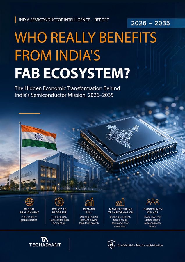
India’s flagship programme — the India Semiconductor Mission, backed by a fiscal envelope first announced at roughly ₹76,000 crore and subsequently broadened — was designed precisely to underwrite this surrounding system, offering support across fabrication, display, compound semiconductors, packaging and design. The policy architecture implicitly concedes the point this report makes explicit: the chip is the smallest part of the problem.
02 — The buildWhat India is actually building
Strip away the framing and the early portfolio is clear. The announced projects cluster around two categories: mature-node and specialty fabrication, and back-end assembly, test and packaging. Tata Electronics’ fab in Dholera, in partnership with Taiwan’s Powerchip (PSMC), targets mature and specialty nodes rather than the bleeding edge. The larger number of projects, however, sit in the back end: Micron’s assembly and test facility in Sanand, Tata’s packaging plant in Assam, and OSAT investments from players such as CG Power and Kaynes.
This is not a shortcoming; it is the textbook entry strategy. Mature nodes and packaging are where most of the world’s chips by volume are actually made, where capital intensity is lower, where ramps are faster, and where a new manufacturing economy can build the operational muscle a future leading-edge ambition would require. The realistic near-term story is therefore an industrialisation story, not a frontier-technology story.
03 — StructureThe dependency stack
Treat the cluster as a graph (Fig. 1). At the centre sits the fab or packaging line. Radiating outward are the dependencies that determine whether it can run at competitive yield and cost: ultrapure water and firm power on the utility side; substrates, photoresists, specialty gases and chemicals on the materials side; bonded logistics and customs throughput; capital; policy stability; and the deepest constraint of all, process talent.
The instructive feature of the graph is that the high-value, high-risk edges point outward and abroad. The tools come from a handful of global equipment makers. The materials come from established suppliers concentrated in East Asia. In the early years, the cluster is a node that imports most of its critical inputs and exports a manufacturing service. Localisation of those edges — not the existence of the node — is the real measure of ecosystem maturity.
Unlock the complete report
You’re reading the free preview. The full analysis continues with six more sections and the downloadable PDF edition.
- 🔒04 · Water, power & land
- 🔒05 · The packaging layer
- 🔒06 · Who captures the value
- 🔒07 · The talent constraint
- 🔒08 · Second-order effects
- 🔒09 · What to watch · references
You’ll be asked to sign in, then complete a one-time secure purchase.