
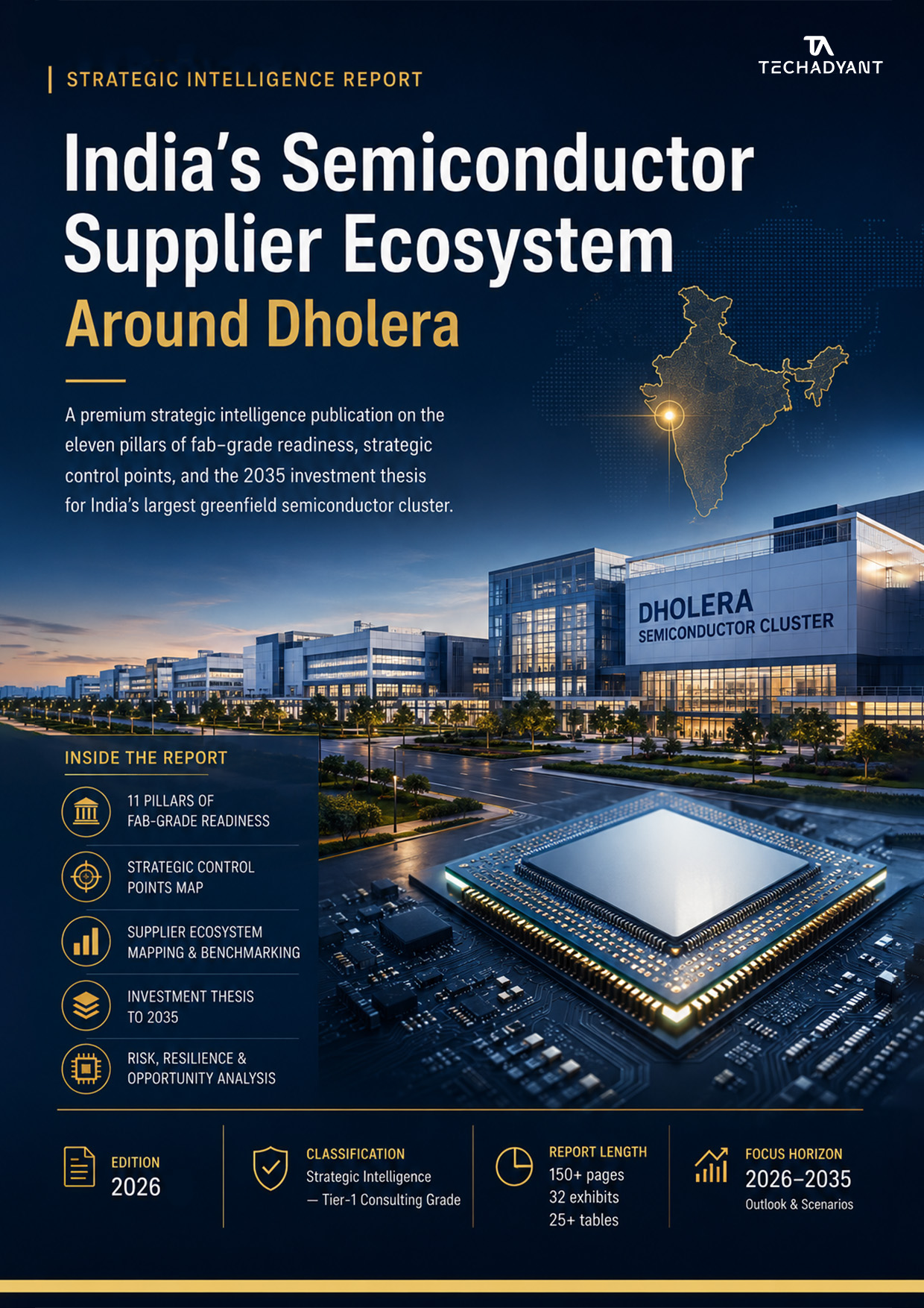
Dholera is the most consequential unfinished node in India’s semiconductor strategy. The Tata Electronics–PSMC fab, the ISM-approved project stack, and the Gujarat semiconductor policy create a credible anchor. What they do not yet create is a self-reinforcing supplier ecosystem. This report is a component-level readiness assessment across wafer-fab equipment, bulk gases and chemicals, photoresists and substrates, packaging-and-testing infrastructure, wafer handling, metrology, logistics, power, water, and the policy levers that determine whether the node produces an industrial cluster or a capital-and-land headline.
- The value is not in the fab alone. Packaging, materials, equipment subcomponents, testing, logistics, power and water constitute the larger share of supplier opportunity and the larger share of current import dependency.
- Localisation is uneven. OSAT/ATMP and mature-node backend segments show more buildable depth than front-end wafer-fab materials and high-purity consumables.
- Industrial policy, continuous power, ultrapure water, logistics connectivity and process skills are now the binding constraints, not capital commitment.
- The ten-year addressable opportunity in Gujarat-linked semiconductor supplier segments is modelled at roughly ₹28,000–62,000 crore, with a faster path through packaging, testing, gases, automation and logistics than through front-end materials.
The India Semiconductor Mission is real, financed, and underway. What remains under-narrated is the supplier map beneath the headline projects. A fab is the visible apex; the cluster is decided by everything around it — bulk gases, chemicals, substrates, photoresists, cleanroom equipment, wafer handling, metrology, packaging substrates, logistics, power, water, and the skills base that keeps yield competitive. This report maps those layers for Dholera and the broader Gujarat supplier catchment.
01 — AnchorDholera as an industrial node
Dholera sits at the intersection of three durable advantages: designated manufacturing land, a state-level semiconductor incentive framework, and proximity to ports and downstream electronics demand. The Tata Electronics–PSMC fab anchors the node with a mature-node, high-volume logic footprint rather than a leading-edge demonstration. That matters because mature nodes are where the world’s chip volume actually runs, where capital intensity is lower, and where supplier localisation is structurally more achievable.
The ISM portfolio adds complementary back-end weight: OSAT and ATMP facilities, compound-semiconductor units, and downstream packaging capacity. Together they create demand signals for the chemicals, materials, precision components and automation that a standalone fab would not generate. The missing piece is the supplier response, especially in front-end materials and equipment subcomponents where domestic capability is thin.


02 — BuildWhat India is actually building
The early portfolio clusters around two categories: mature-node and specialty fabrication, and back-end assembly, test and packaging. That is not a shortcoming; it is the textbook entry sequence. The larger opportunity sits in the supplier layers that make these nodes commercially viable at competitive yield and cost.
Wafer-fab equipment, specialty gases, high-purity chemicals, photoresists, substrates, cleanroom hardware, bonded logistics, and metrology are still import-led. Domestic capability exists in pockets — specialty gases, electronics chemicals, some cleanroom integration — but not at the volume, purity and qualification standards a high-volume fab demands. Packaging and testing show more domestic content because India already hosts mature assembly operations and equipment localisation is easier than chemical-process localisation.


03 — Supplier stackLayers, gaps and readiness
Readiness varies sharply by layer. Gases and chemicals show the highest volume demand and the lowest domestic substitution rate outside standard industrial grades. Metals and wafer-handling consumables have more Indian engineering content but still depend on imported upstream intermediates. Metrology is both the most difficult to localise and the most yield-sensitive; Indian capability is concentrated in instrument integration rather than detector or source manufacturing.
Logistics, warehousing and bonded transport are underappreciated chokepoints. A fab importing 20–30 specialty SKUs with short shelf life and strict storage requirements needs more than port access; it needs cold-chain-grade chemical logistics, quarantine capacity, and vendor-managed inventory close to the site. Gujarat has port adjacency; it does not yet have the specialized logistics catchment a semiconductor-grade supplier park would require.


04 — ConstraintsWater, power, policy and talent
Capital is no longer the binding constraint; the India Semiconductor Mission has de-risked the investment decision for anchor projects. The binding constraints are now physical and institutional: ultrapure water at fab-grade volumes and consistent quality; firm, dedicated power with low outage frequency; logistics readiness for high-value chemical inputs; and process engineering talent at scale.
Water is the most acute near-term constraint. A 28–110 nm fab cluster will demand multiple million litres per day of ultrapure water, with rejected streams that require treatment before reuse or discharge. Gujarat’s water budget, seasonal variability, and the interaction between industrial, agricultural and urban demand need explicit allocation and recycling targets. The report models the water arithmetic for a Dholera-scale cluster and maps the policy levers that close the gap.
Talent is the longer-cycle constraint. Semiconductor process engineering, cleanroom operations, materials QA, and equipment maintenance require multi-year curricula and hands-on exposure that India currently provides at a fraction of the required scale. The near-term bridge is hiring returnee talent, importing technician training programmes, and partnering with equipment makers for on-site capability transfer.


05 — CatchmentGujarat and the broader domestic base
Dholera’s domestic supplier catchment is not limited to Gujarat. The report assesses supplier readiness across Maharashtra, Tamil Nadu, Karnataka, Telangana and Delhi-NCR — the states that already host the bulk of India’s electronics manufacturing, industrial gases, chemicals, precision engineering and logistics capability. The conclusion is that political commitment to Dholera needs to be matched by an equally explicit supplier-park and logistics framework if the node is to avoid becoming a fab island surrounded by import-dependent supply chains.


06 — PriorityWhere capital creates the most optionality
Not all supplier opportunities are equally investable today. The report ranks surfaces across three dimensions: capital intensity, time to revenue, and import-dependency severity. The highest-priority surfaces for the 2026–2030 window are packaging substrates, high-purity gases, wafer-handling consumables, test equipment integration, logistics enclaves, captive power and raw-water recycling infrastructure. Longer-horizon plays include photoresist manufacturing, coater-developer localisation, and advanced metrology subsystems.


07 — Watch listScenarios, signals and decision thresholds
The report closes with three scenarios for Dholera’s supplier ecosystem evolution through 2035: a Base case in which announced policy instruments are implemented on schedule and supplier localisation proceeds at historical Indian industrial rates; an Accelerated case in which targeted co-investment, logistics parks and skills academies compress the timeline; and a Constrained case in which water allocation disputes, power interconnection delays and equipment qualification bottlenecks leave the fab operational but ecosystem formation lagging by seven to ten years.
The decision thresholds are practical: if domestic gas and chemical capability is not at pilot-production scale within eighteen months of fab tool-in, the risk profile rises sharply. If the Dholera logistics framework does not explicitly include semiconductor-grade chemical warehousing and bonded transport by the time commercial wafers flow, import costs and insurance premiums will understate the true cost of Indian manufacturing.


The full report continues with six additional sections: supplier readiness scores by segment, a 130-page dependency and opportunity map, three scenario models for the Dholera catchment, a 32-figure evidence lattice, eighteen tables, and five appendices with supplier, policy, infrastructure, investment and skills-reference tables. The conclusion is that Dholera can become a genuine semiconductor cluster, but only if supplier policy, water, power, logistics and skills are treated as first-class strategic bets rather than downstream afterthoughts.
Unlock the complete report
You’re reading the free preview. The full analysis continues with six more sections and the downloadable PDF edition.
- 🔒04 · Water, power & land
- 🔒05 · The packaging layer
- 🔒06 · Who captures the value
- 🔒07 · The talent constraint
- 🔒08 · Second-order effects
- 🔒09 · What to watch · references
You’ll be asked to sign in, then complete a one-time secure purchase.