
Semiconductor Ecosystems
Techadyant Labs research on semiconductor ecosystems in India — the dependencies, constraints and opportunity surfaces that decide the real outcome. 2 published reports.
 ₹5,900
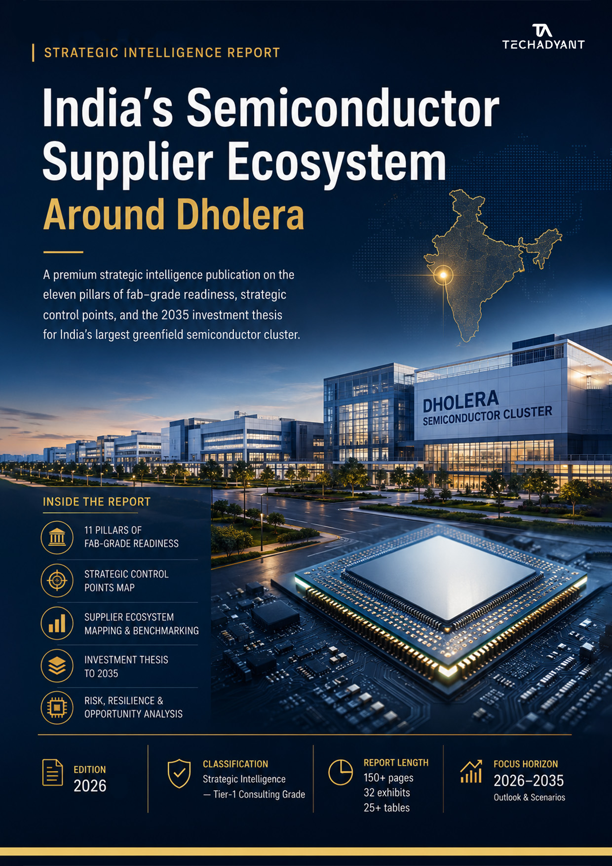
India's Semiconductor Supplier Ecosystem: The Dholera Play
Mapping the supplier stack, anchor investments and build-ready parts for Dholera as a fab-led industrial node.Dholera is being positioned as India's anchor fab-led industrial node, but supplier ecosystem readiness is only partially mapped. This report moves from announcement-stage coverage to component-level readiness assessment across wafer fabrication equipment, bulk gases and chemicals, photoresists and substrates, packaging-and-testing infrastructure, materials handling, power and water utilities, and the policy levers that determine whether a project becomes a production node rather than a land-and-incentive headline. It maps India's existing semiconductor manufacturing base—Tata Electronics fab at Dholera, ISM-approved projects, OSAT/ATMP facilities, compound-semiconductor units, packaging clusters and downstream electronics demand—against the actual supplier presence in Gujarat and the broader domestic base. The core finding is that localisation is uneven: packaging-and-testing and mature-node backend segments show more buildable supplier depth than front-end wafer fab materials, equipment subcomponents and high-purity consumables. Industrial policy, continuous power, ultrapure water, logistics connectivity and skills availability are now the binding constraints, not capital commitment alone. The report scores supplier readiness by segment, identifies the highest-value localisation opportunities, names the import-dependent chokepoints, and lays out a phased industrial-policy and infrastructure agenda for converting Dholera from a fab site into a self-reinforcing semiconductor supplier ecosystem. 96 pages, 34 figures, 18 tables, 5 appendices with supplier, policy, infrastructure and investment reference tables.
 ₹4,900
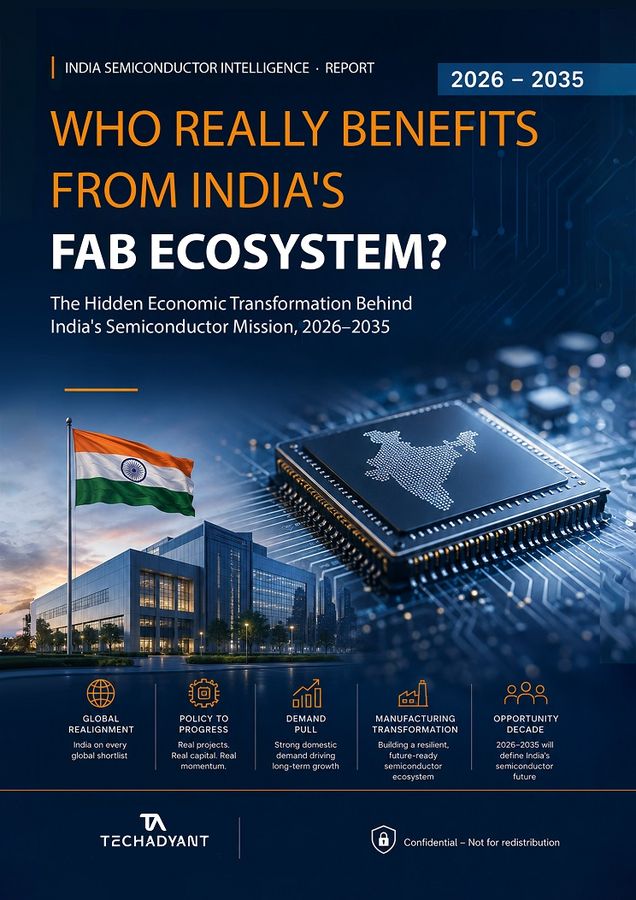
Who Really Benefits from India’s Fab Ecosystem?
The Hidden Industrial Transformation Behind India’s Semiconductor MissionIndia’s semiconductor push is usually told as a story about chips. It is better understood as a story about land, water, power, packaging and people — and about who captures the value when a state decides to manufacture its way up the technology stack.
Front-end fabrication attracts the headlines, but the binding constraint on near-term output is back-end assembly, test and packaging capacity — and the specialised inputs it quietly depends on.
Kerala’s NetraSemi, backed by Zoho, has unveiled the A2000 — a 12nm edge-AI system-on-chip and the first Indian-designed AI chip to reach silicon. It matters less as a product than as proof of a thesis: edge AI is the one layer of the AI-hardware stack India can contest now, without a leading-edge fab.
Of a ₹91,000 crore mature-node fab, roughly two-thirds flows to ASML, AMAT, Lam, TEL and KLA. The Indian-capture economy lives in the remaining one-third — construction, gases, UPW, logistics and the durable industrial capabilities those build.
Most coverage will lead with the Rs 1.27 lakh crore. The real story is one sentence - "building the complete ecosystem" - and a second pillar that finally incentivises the machines, materials, chemicals and gases beneath the fab.
Gallium, germanium, electronic-grade chemicals and high-purity targets are the quiet dependencies beneath every fab. China already accounts for the dominant share of refining; India is building the demand side without the supply base.
Marvell will invest US$250 million over the next three years to expand technology, talent and infrastructure in India. The announcement is less about real estate than about concentrating advanced chip-design capability in India — architecture, ASIC design, verification, AI accelerators and cloud networking silicon.
IC substrates are one of the few layers where India has no producer at all and three firms hold ~70% of the world market. The first plant to address it — Intel and 3DGS, US$3.3bn in Odisha — is building glass-core substrates, a technology nobody has in volume production anywhere. India is entering this layer at the frontier rather than a generation behind. It is also entering it as a host, not an owner.
PM Modi laid the foundation for ASIP Technologies' Rs 2,500 crore OSAT plant in Visakhapatnam — South India's first ISM-approved chip unit, and a step down the value chain from design into physical manufacturing.
L&T Semiconductor Technologies (LTSCT) is shifting its outsourced assembly and testing (OSAT) operations from overseas facilities to India, partnering with domestic providers including Tata Electronics - a step in localising the semiconductor backend supply chain.
Gujarat, through the Gujarat State Electronics Mission (GSEM), is setting up a ChipIN Extension Centre and a Centre of Excellence for VLSI Design with Gujarat Technological University (GTU) and C-DAC - a move to build state-level chip-design capability beyond fabrication and assembly.
Uttar Pradesh has secured investment commitments exceeding Rs 45,000 crore from eight companies across semiconductor, electronics and renewable-energy sectors, concentrated in Gautam Buddha Nagar. HCL-Foxconn's India Chip Pvt. Ltd. will invest Rs 3,706 crore in a semiconductor unit, and Ascent Circuits Rs 3,250 crore for PCBs and semiconductor substrates.
Prime Minister Narendra Modi announced from the Red Fort on 15 August 2026 that three major semiconductor plants are already operational in India, with an additional five to eight plants expected to come online over the next seven to eight years.
Chennai-based Aheesa Digital Innovations achieved first-pass silicon success with VIHAAN, an indigenous broadband networking System-on-Chip built on the VEGA microprocessor, on 15 August 2026. Production tape-out is targeted for 2027.
MeitY Secretary S Krishnan announced on 18 August that three semiconductor facilities — Micron, Kaynes and CG Semi, all at Sanand in Gujarat — have entered commercial production under ISM 1.0, with five to six projects expected to be live by end-2026. The Union Cabinet has approved ISM 2.0 with an outlay of Rs 1,27,500 crore, and PM Modi will inaugurate SEMICON India 2026 on 17 September.
MeitY approved 31 new Electronics Component Manufacturing Scheme proposals worth Rs 7,877 crore on 17 August, lifting total sanctions to 106 projects representing Rs 69,548 crore of investment and projected production of Rs 5.34 lakh crore across 15 states.
Electronics Minister Ashwini Vaishnaw has laid out the detailed implementation roadmap for Semicon 2.0, targeting 7nm-to-3nm chip technology within eight years and the training of 100,000 semiconductor design engineers. The plan marks a shift from fabrication-focused incentives toward a broader ecosystem spanning chip design, manufacturing equipment, materials, advanced packaging and talent.
DRDO has developed indigenous gallium nitride (GaN) technology for next-generation radar and electronic warfare, built on silicon-carbide wafer processes at the Solid State Physics Laboratory. Reporting cites a single 3.5 x 3 mm GaN chip delivering up to 30 W — compound semiconductors, not logic fabs, are where several defence import dependencies actually sit.
About $1.4 billion in cumulative equity has gone into 281 Indian semiconductor-related companies, roughly half of it since 2025, days before SEMICON India 2026 opens in New Delhi. Investor cheques are a harder signal than policy outlays of whether design, OSAT, materials and equipment stories are actually investable.
US chip-equipment major Applied Materials will invest about Rs 3,600 crore in Karnataka over roughly a decade for semiconductor R&D, equipment manufacturing and software, with a signed MoU and about 140 acres allotted in Bengaluru. The tools-and-process layer, not another fab, is the part India most needs to build.
A day before SEMICON India 2026 opened, PM Modi chaired a roundtable with the heads of ASML, Applied Materials, Lam Research, Tokyo Electron, Micron, Infineon, AMD, Intel and Tata Electronics. With twelve units approved and Semicon 2.0's Rs 1,27,500 crore notified, the next test is whether the equipment, materials and design majors embed deep local capability rather than remain arm's-length suppliers.
Lam Research will invest about Rs 10,000 crore in India for its first silicon-component manufacturing facility and an R&D expansion - a global process-equipment major moving into the tools-and-materials layer that India still imports almost entirely, and the part of the stack that packaging and mature-node fabs do not fix.
On SEMICON India 2026's opening day, minister Ashwini Vaishnaw said Semicon 2.0 has drawn about Rs 1 lakh crore (USD 11-12 billion) in commitments - weighted toward equipment, materials, gases, chemicals and substrates rather than more fabs, across 16 MoUs and announcements. It is a commitment pipeline, not contracted capital, but its composition is the structural signal: the money is finally moving upstream of the fab.
Applied Materials used SEMICON India 2026's opening day to unveil India Vision 2035 - a USD 5 billion, ten-year commitment built around a 140-acre advanced semiconductor research park and a tenfold expansion of its India supply-chain base. It is a far bigger bet than its Rs 3,600 crore Karnataka MoU days earlier, and it lands in the tools-and-process layer India still imports almost entirely.
At SEMICON India 2026, Tata Electronics signed MoUs to build a 363-acre vendor park around its Dholera fab (with Ascendas First Space) and to localise critical inputs - Fujifilm's roughly Rs 800 crore materials plant, JSR's photoresists and chemicals, plus Nexperia, BESI and SCL. It is the first concrete attempt to populate the supplier layer that has to sit around India's largest silicon project.
On SEMICON India's Day 2, Tata Electronics signed MoUs with INOX Air Products for high-purity semiconductor gases and with Sumitomo Chemical for wet chemicals and advanced materials. A fab needs more than 50 ultra-high-purity gases and hundreds of specialty chemicals, most still imported - the continuous-consumption layer that packaging and even silicon capacity do not fix.
SEMICON India 2026 closed on 19 September with a harder signal than its 56 MoUs: the PM inaugurated commercial production at CDIL Semiconductor (Mohali) and Suchi Semicon (Surat), taking operational units among the twelve Semicon 1.0 projects from three to five. Commercial production is the part of India's chip story that cannot be walked back.
ASML, the sole supplier of high-end lithography tools, has begun operations in India and plans to hire an initial 20-30 engineering graduates, executives said around SEMICON India 2026. The office is framed as customer support and talent access ahead of Tata Electronics' planned 300 mm fab - not equipment manufacturing. It marks the lithography layer's first onshore footprint, even as the tools themselves stay imported.
Linde India has secured a land parcel in Sanand, Gujarat, for a semiconductor packaging-gas facility - its second India chip-gas site after the Dholera plant set to supply Tata''s fab. Electronic specialty gases are a real, under-noticed chip dependency; the supply is being localised, but largely by global majors - which brings the molecule onshore without yet localising the technology or the ownership.
The Technology Development Board under DST has signed a Rs 130 crore agreement with Bengaluru's BigEndian Semiconductors for Project VeerAI, a Rs 260 crore camera-focused AI vision system-on-chip meant to move from TRL-5 to TRL-9. The first market is secure CCTV and surveillance. It is development funding, not production, and the process node and timeline were not disclosed.
Map this ecosystem
See where India stands across the value chain — players, dependencies and scores — in the free Atlas.